
Powerplan 做什么
工艺:T12nm(12nm ARM A55)
阶段:Power planning
类型:方法口径 / 经验记录
口径
电阻计算公式
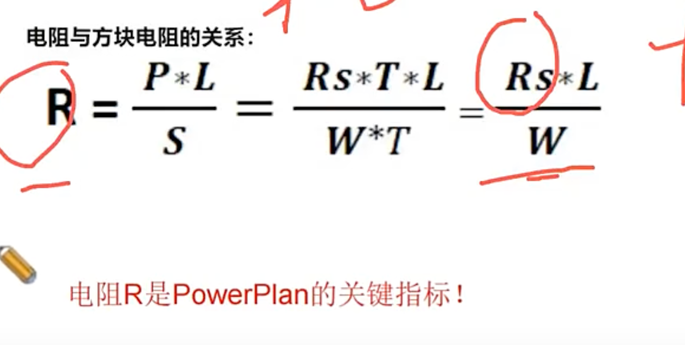
R:电阻 Rs:方块电阻 L:长度 W:横截面
Powerplan 做什么?
创建从芯片供电源头到各个 cell、PG pin 的供电通路。
在 T12nm 中,powerplan 的结构是:M1 和 M2 是 power rail,并联 dual rail(du rail)。 为什么要做 dual rail?
M1和M2的线宽小,使用dual rail 并联,电阻能变小,从而改善IR Drop
在T12nm中也使用了Via Pillar, 为什么要用Via Pillar?
Via Pillar 本质也是通过 并联让电阻变小,从而改善IR Drop
double patterning
在T12nm中 M1 - M3 都是 double patterning,有2张mask;因此做powerplan的时候没有添加 via1(会有spacing问题),需要到chipfinish阶段时才会添加 via1
T12nm Metal(1P11M)
本项目用 1P11M(1 层 Poly + 11 层 Metal):
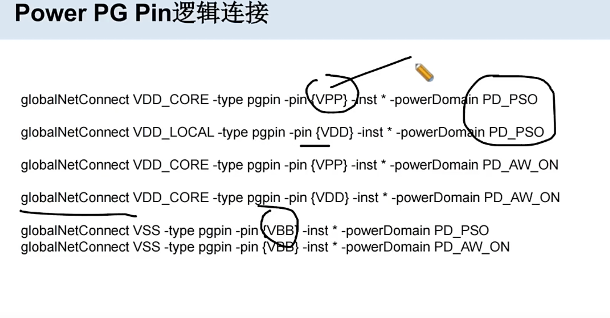
Domain 的 逻辑连接
Power Switch Domain
- VDD -> VDD_LOCAL
- VPP -> VDD_CORE
- VSS -> VSS
- VBB -> VSS
Power Always On Domain
- VDD -> VDD_CORE
- VPP -> VDD_CORE
- VSS -> VSS
- VBB -> VSS
VPP:N-well 连接 的 PG pin
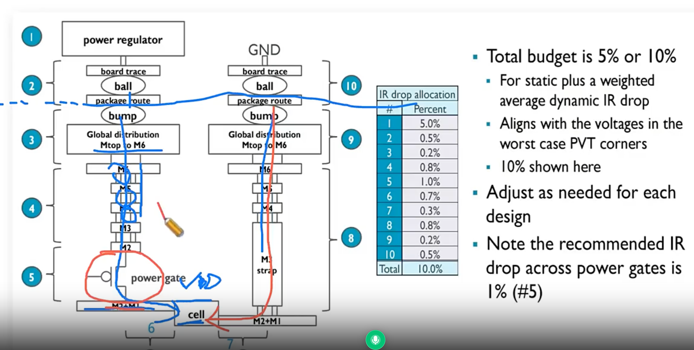
供电路径总览(结合 Power Switch)
名词对号入座
一句话:高层从M9 把 global 电(VDD_CORE)打到power switch 的 TVDD → power switch 这道闸决定哪片区域有电 → 闸后变成 VDD_LOCAL,std cell 走 M1/M2 双轨、memory 走自己的 M5 stripe 拿电。
Core区域 的供电结构(T12nm)
M9 的 VDD_CORE -> 打到M1的power switch -> pso 开启后 -> TVDD 拿到电 -> 相邻的 VDD_LOCAL 拿到电
core区域其它的rail如何拿到电?
T28nm通过 mesh 网络结构拿到, T12通过 via pillar 反供从而使得core区域其它rail也拿到电
core区域的 Tapcell 的 VPP 连接到 VDD_CORE, VDD 连接到 VDD_LOCAL
Memory 的供电结构(T12nm)
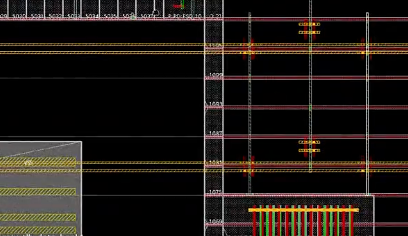
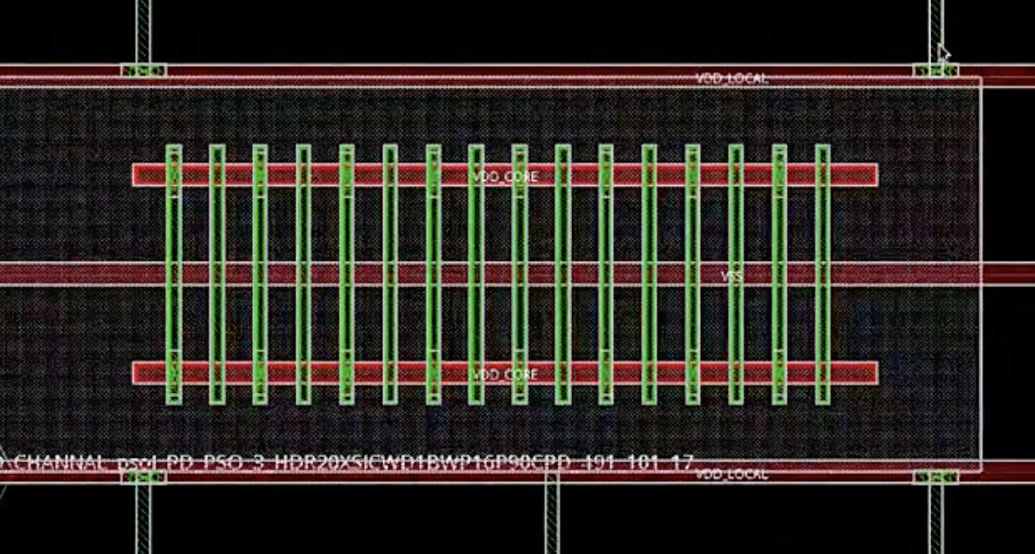
回答版:Global VDD → TVDD → switch打开 -> VDD_LOCAL 的power rail -> 通过 via pillar 反供到高层去,然后在送进memory中
理解版:
Memory 的pin 在M4, 连接到M6出去, M6拉出去就近找到PowerSwitch(在这个过程中是先通过 Via Pillar 连接到外面 Pillar 的M3,然后连接到 power switch所供的 VDD_LOCAL )
物理连接(从 Memory 往回看):
即:switch 打开后 VDD_LOCAL 从低层 rail 经 pillar 反爬到 M6/M5 高层,再打孔逐层送进 Memory 的 M4 pin。
注记: 此处口径为 Global VDD → TVDD → switch(输入侧);与上文「Power Switch 与高低层」中 VDD_CORE → switch 的表述并存,具体网名以项目 UPF / def 为准。
说明
- UPF 先把功耗意图(domain / net / switch 等)交给工具;Powerplan 再在物理上把供电从源头接到每个单元与 PG 脚。
- 典型包括 ring、mesh、stripe、via 叠层,以及接到 std cell / macro 的 PG pin(含 local 如
VDD_LOCAL)。 - 本项目路径:高层 VDD_CORE → Power switch → 低层 M1/M2 的 VDD_LOCAL → Memory / cell。Switch 侧电源名为 TVDD、VDD_LOCAL、VSS。
并联 dual rail 是什么?
Dual rail = 电源/地那套供电双轨;并联 = 同一供电在 M1、M2 两层一起走、via 连上,不是只靠单层。
Q:Primary PG / Secondary PG 是什么?
需要 Secondary PG 的典型 cell:power switch(gate 驱动要常供电)、isolation cell(钳位电源常在)、retention register(备份状态 always-on)、always-on buffer / enable level shifter、tap cell(well tap,secondary PG pin 为 VPP)。
对应本项目:高层 VDD_CORE / TVDD 这类常供电网络接到这些 cell 的 secondary pin,普通 std cell 只接 M1/M2 的 VDD_LOCAL(见上文「Power Switch 与高低层」)。
T12nm 中 tap cell 的 secondary PG pin(VPP)逻辑连接到 VDD_CORE。 脚本佐证:power_stape_pso 图 1 先按 domain 连(PD_AW_ON 域 VPP→VDD_CORE、PD_PSO 域 VPP→VDD_LOCAL);随后 Innovus 03 Powerplan 图 3 对 *VPP_VSS cell(tap cell)先 setPGPinUseSignalRoute 让 VPP 走 signal route,再 globalNetConnect VDD_CORE -type pgpin -pin VPP ... -override 统一重连到 VDD_CORE。
Core 区域 cell 的电源连接结构(物理): tapcell 的连接即是 std cell 的连接——从 VPP 出发往上层,接到 power switch 附近的 pillar,之后连接 power switch:
pillar 即 power switch cell 上的 stapling / via pillar,其创建脚本见 power_stape_pso。